How pcb vias are made
Oct 29, 2022
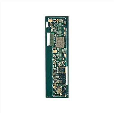
Vias, holes on the circuit board, connect the lines between different layers, and change the circuit board from a planar structure to a three-dimensional structure.
It is too difficult to avoid crossing of single-layer lines, and double-layer or more lines must be connected through vias. Through the copper on the hole wall, the circuit copper wires of the upper and lower layers are connected.
Single-layer PCB, sometimes it is impossible to route, and the layers must be changed through vias. Large and small vias to connect circuits on different layers
What types of vias are there?
There are two types of vias on the circuit board: mechanical holes and laser holes.
(1) Mechanical hole: a hole drilled with a mechanical drill. The inner diameter of the hole is more than 0.2 mm. A bigger hole will be drilled with a thicker drill bit. Consumer electronic products are usually designed with an inner diameter of 0.3mm. Ordinary circuit board manufacturers can make 0.3mm mechanical holes. If the mechanical holes of 0.2mm and 0.25mm are used, the drill bit will be easy to break due to the slow drilling speed, and the price will be more expensive. Not all PCB manufacturers can make such small mechanical holes. The drill bit drills through the circuit board at once, so the mechanical hole is also called a through hole.
(2) Laser hole: a hole punched by a laser. The inner diameter is generally 0.1mm. There are few laser holes of other specifications. Because the power of the laser is limited, it cannot directly penetrate the multi-layer PCB board, and is usually used as a blind hole on the surface.
Considerations for PCB Via Design
(1) The aperture should be as large as possible: as mentioned above, small drills should be used for small holes. Small drills are expensive and have high requirements for the board factory. If the board area is large, even 0.5mm inner diameter mechanical holes can be used.
(2) Try not to use laser holes: that is, try not to use laser holes. The circuit board with one layer of laser holes is 30% more expensive than the one without laser holes (first order board). The one with 2 layers of laser holes is 30% more expensive than the one with 1 layer of laser holes (second-order board).
(3) Other more expensive designs: The more complicated the via process is, the higher the price of the circuit board is, and the difference between the cheapest and the most expensive is more than tens of times. For example, a 0.2mm mechanical hole is about 20% more expensive than a 0.3mm mechanical hole circuit board; a stacked hole board with overlapping 2-layer laser holes is more than 20% more expensive than a staggered-hole board with 2 layers of laser holes staggered; Apple mobile phone likes to use any layer interconnection The board is more than 10 times more expensive than ordinary circuit boards with only mechanical holes (the whole board is overlapped with laser holes).
Dense punching, regular arrangement or random arrangement?
The inner surface area of each via is limited, and the current through it is also limited.
For power lines, ground lines and other PCB lines that need to pass a large current, many vias need to be punched.
Random punching and regular punching
These vias can be arranged regularly in a matrix, or they can be arranged randomly. Is there any difference between the two?
Regular arrangement looks better than random arrangement. Randomly arranged drawings are fast. Most companies do not have mandatory requirements, and PCB engineers with "obsessive-compulsive disorder" prefer to use rules.
Matrix-type regularly arranged vias may be more capable of blocking signals in certain directions. If you don't deliberately chase them to look good, random punching will be more secure.