


FR4 Material Multilayer Pcb
FR4 material multilayer pcb refers to multilayer circuit boards used in electrical products, and multilayer boards use more single-sided or double-sided wiring boards.
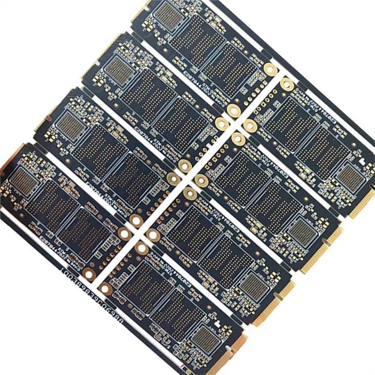
Description
Product Detail
FR4 material multilayer pcb came into being for the ever-changing changes in the electronics industry. Over time, the functions of electronic devices have gradually become more and more complex, requiring more complex PCBs.
Product name: FR4 material multilayer pcb | Type:Rigid board |
Place of original:China | Brand name: Beton |
Copper thickness:1 OZ | Solder mask color: Black |
Silkscreen: White | Material: Fr4 |
Application: Consumer electronics | Supply type:PCB, PCBA, FPC, HDI, Rigid-flex PCB |
Deliver time:7-10 days | Certificate:ROSH, ISO9001, UL |

The structure of FR4 material multilayer pcb is as follows:
1. Signal layer
AlTium Designer provides up to 32 signal layers, including top, bottom, and middle layers. The layers can be connected to each other through vias, blind vias and buried vias.
(1) Top signal layer
Also known as the component layer, it is mainly used to place components. For double-layer boards and multi-layer boards, it can be used to arrange wires or copper cladding.
(2) Bottom signal layer
Also known as the solder layer, it is mainly used for wiring and soldering, and can be used to place components for double-layer boards and multi-layer boards.
(3) Intermediate signal layer
There can be up to 30 layers, which are used to arrange signal lines in multi-layer boards, excluding power lines and ground lines.
2. Internal power layer
Usually referred to as the inner electrical layer, it only appears in multi-layer boards. The number of PCB board layers generally refers to the sum of the signal layer and the inner electrical layer. Similar to the signal layer, the interconnection between the inner electric layer and the inner electric layer and between the inner electric layer and the signal layer can be realized by through holes, blind holes and buried holes.
Advantages of FR4 material multilayer pcb
From a technical point of view, multilayer PCBs offer several advantages in terms of design. These advantages of multilayer printed circuit boards include:
1. Small size: One of the most prominent and praised benefits of using multilayer printed circuit boards is their size. Due to its layered design, the multilayer PCB itself is smaller than other PCBs with similar functions. This brings huge benefits to modern electronics as the current trend is towards smaller, more compact yet more powerful gadgets such as smartphones, laptops, tablets and wearables.
2. Lightweight structure: With a smaller PCB, the weight is lighter, especially because the multiple connectors required for the interconnection of single-layer and double-layer PCBs are eliminated, which is beneficial to the multi-layer design. This again is good for modern electronics, which are more inclined towards mobility.
3. High quality: Due to the amount of work and planning that has to be done when manufacturing a multilayer PCB, these types of PCBs tend to be better than single and double layer PCBs. Therefore, they are also more reliable.
4. Improve durability: Multilayer PCBs tend to be durable by their nature. Not only must these multilayer PCBs hold their own weight, but they must also be able to handle the heat and pressure used to bond them together. In addition to these factors, multilayer PCBs use multiple layers of insulation between circuit layers, binding them together with prepreg adhesives and protective materials.
5. Increased flexibility: While this does not apply to all multilayer PCB assemblies, some do employ flexible construction techniques, resulting in flexible multilayer PCBs. This can be a very desirable characteristic for applications where slight bends and bends may occur on a semi-regular basis. Again, this does not apply to all multilayer PCBs, and the more layers you add to a flex PCB, the less flexible the PCB will be.
6. More powerful: Multilayer PCBs are extremely high-density components that combine multiple layers into a single PCB. These close proximity make circuit boards more connected, and their inherent electrical properties allow them to achieve greater capacity and speed, albeit in a smaller size.
FAQs
Q1:Are you a factory or trade company?
A: Yes, we are the factory, we have our own PCB manufacturing & Assembly factory.
Q2:What kind of PCB file format can you accept for production?
A:Gerber, PROTEL 99SE, PROTEL DXP, POWER PCB, CAM350, GCCAM, ODB+(.TGZ)
Q3:Are my PCB files safe when I submit them to you for manufacturing?
A:We respect customer's copyright and will never manufacture PCB for someone else with your files unless we receive written. Permission from you, nor we'll share these files with any other 3rd parties.
Q4:No PCB file/Gbr file, only have the PCB sample,can you produce it for me?
A: Yes,we could help you to clone the PCB. Just send the sample PCB to us, we could clone the PCB design and work out it.
Q5:What is Chuante lead time?
A:Sample:
1-2 Layers: 5 to 7working days
4-8 Layers: 12 working days
Mass production:
1-2 Layers:7 to 15 working days
4-8 Layers:10 to 18 working days
The lead time depends on your final confirmed quantity.
Hot Tags: fr4 material multilayer pcb, China, suppliers, manufacturers, factory, customized, buy, cheap, quotation, low price, free sample


