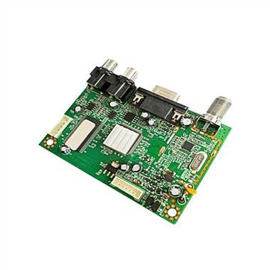
HDI PCB Printed circuit board
Beton HDI technology can meet customers' product requirements. The HDI PCB we produce uses full digital signal processing technology and a number of patented technologies. It has a full range of adaptive load capacity and strong short-term overload capacity.
Description
Product Detail
Item | Specification |
Material | FR-4,FR-2,CEM-1,CEM-3,Carbon,Rogers,etc |
Remarks | High TG CCL is Available |
Finish Board Thickness | 0.3mm-6.00mm |
Production technology | HDI |
Surface Finish | Solder Mask(black, green, white, red, blue, ) Silkscreen(black, yellow, white) |
Copper Thickness | 1/2 oz min,12oz max |
Shape | Routing, Punch,V-cut |

The denefition of HDI board
High Density Interconnect (HDI) circuit boards are printed circuit boards with high wiring density per unit area. In general, HDI PCBs are defined as all PCBs: microvias; blind and buried vias; build-up and high signal performance. Printed circuit board technology is constantly changing and evolving, with product requirements smaller and faster. HDI boards are more compact, with less vias, pads, copper traces, and less space. So, HDI is a denser wiring, lighter, more compact PCB with fewer layers. Instead of using several PCBs in a device, a single HDI board can accommodate the functionality of previously used boards.
The benefit of HDI board
HDI printed circuit boards can be continuously improved with copper etching technology for higher precision, and the functions of multiple PCBs can be combined into one HDI PCB, so there are the following advantages:
Low cost: If planned properly, the overall cost can be reduced compared to standard PCB due to fewer layers required, smaller size/number of boards required.
Shorter lead times: Design efficiencies in HDI PCB production mean faster lead times. HDI is easier to place components and vias, as well as electrical performance, so it takes less time to complete the design and test process of an HDI PCB.
High reliability: Microvias have better reliability than typical through-holes due to the use of a smaller aspect ratio; they are more reliable than through-holes, giving HDI outstanding performance with better materials and parts.
Quality:
IPC-600G classⅡand IPC-6012B classⅡstandards.
ISO9001:2008 Quality Management
Probe flying test and Electrical test
UL certified Rating 94v-0
X-ray Inspection,
Automated Optical Inspection (AOI)
In-circuit Testing (ICT) and Function testing
ROHS compliance.

Beton FAQS
Q1. What is required for quotation?
Beton: Quantity, Gerber files and technical requirements (material, surface finish treatment, copper thickness, board thickness...) PCB information, BOM, (test files...)
Q2. What file formats do you accept for production?
Beton:
Gerber file: CAM350 RS274X
PCB file: Protel 99SE, P-CAD 2001 PCB
BOM: Excel (PDF,word,txt)
Q3. Are my documents safe?
Beton: Your files will be kept private. We protect our clients' intellectual property throughout the process.
Q4.MOQ?
Beton: No MOQ. We are able to flexibly handle small and large volume.
Q5. Shipping fee?
Beton: The shipping fee is determined by the destination, weight and package size of the PCBs.
Hot Tags: HDI PCB Printed circuit board, China, suppliers, manufacturers, factory, customized, buy, cheap, quotation, low price, free sample