What is impedance control in pcb
Oct 28, 2022
What is a PCB Impedance Board? How to calculate PCB impedance? What is Impedance Control and Impedance Matching?

First, the definition of PCB impedance board
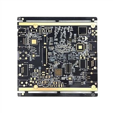
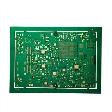
Impedance plates are generally also called impedance strips. A good laminated structure can control the characteristic impedance of the PCB, and its traces can form an easily controllable and predictable transmission line structure called an impedance plate.
Second, the impedance characteristics of the PCB
(1) According to the theory of signal transmission, the signal is a function of time and distance variables, so each part of the signal may change on the connection. Therefore, the AC impedance of the connection is determined, that is, the ratio of the voltage change and the current change is the characteristic impedance of the transmission line: the characteristic impedance of the transmission line is only related to the characteristics of the signal connection itself.
(2) In the actual circuit, the resistance value of the wire itself is less than the distributed impedance of the system, especially in high-frequency circuits, the characteristic impedance mainly depends on the distributed impedance caused by the unit distributed capacitance and unit distributed inductance of the connection. The characteristic impedance of an ideal transmission line depends only on the unit distributed capacitance and unit distributed inductance of the connection.
3. How to calculate PCB impedance
(1) The proportional relationship between the rising edge time of the signal and the time required for the signal to be transmitted to the receiving end determines whether the signal connection is regarded as a transmission line. The specific proportional relationship can be explained by the following formula: If the length of the wire connection on the PCB is greater than l/b, the connection wire between the signals can be regarded as a transmission line.
(2) According to the calculation formula of the signal equivalent impedance, the impedance of the transmission line can be expressed by the following formula: In the case of high frequency (tens of megahertz to hundreds of megahertz), wL>>R (of course, in the range of signal frequency greater than 109Hz) , the skin effect of the signal is considered, and this relationship needs to be carefully studied). Then for a certain transmission line, its characteristic impedance is a constant.
(3) The reflection phenomenon of the signal is caused by the inconsistency of the characteristic impedance of the driving end of the signal and the transmission line and the impedance of the receiving end. For a CMOS circuit, the output impedance of the driving end of the signal is relatively small, tens of ohms. The input impedance of the receiving end is relatively large.
Fourth, the impedance control of the PCB
(1) There will be various signal transmissions in the conductors in the circuit board. In order to increase the transmission rate, the frequency must be increased. If the circuit itself is different due to factors such as etching, stack thickness, and wire width, the impedance value will change. , distorting its signal. Therefore, the impedance value of the conductor on the high-speed circuit board should be controlled within a certain range, which is called "impedance control".
(2) The main factors that affect the impedance of PCB traces are the width of the copper wire, the thickness of the copper wire, the dielectric constant of the medium, the thickness of the medium, the thickness of the pad, the path of the ground wire, the trace around the trace, etc. . Therefore, when designing the PCB, it is necessary to control the impedance of the wiring on the board, so as to avoid signal reflection and other electromagnetic interference and signal integrity problems as much as possible, and ensure the stability of the actual use of the PCB board. The calculation method of microstrip line and strip line impedance on the PCB board can refer to the corresponding empirical formula.
5. Impedance matching of PCB
(1) In the circuit board, if there is a signal transmission, it is hoped that it can be smoothly transmitted to the receiving end with the minimum energy loss from the sending end of the power supply, and the receiving end will completely absorb it without any reflection. To achieve this kind of transmission, the impedance in the line must be equal to the impedance inside the sending end, which is called "impedance matching".
(2) When designing high-speed PCB circuits, impedance matching is one of the elements of the design. The impedance value has an absolute relationship with the routing method. For example, whether to walk on the surface layer or the inner layer, the distance from the reference power supply layer or ground layer, the width of the trace, the material of the PCB, etc. will all affect the characteristic impedance value of the trace.
(3) That is to say, the impedance value can only be determined after wiring. Generally, the simulation software will not be able to consider some wiring situations with discontinuous impedance due to the limitation of the circuit model or the mathematical algorithm used. Some terminations, such as series resistors, can be reserved to mitigate the effect of discontinuous trace impedance.
But the real solution to the problem is to try to avoid impedance discontinuities when wiring.

The above is the description of the elements of the PCB impedance board. Beton has rich production experience in the field of impedance control and supports impedance control, multi-level impedance, and impedance matching. For PCB needs, please contact sales at linda@pcbsfactory.com.