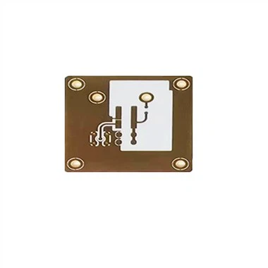
AIN Ceramic PCB
AIN ceramic PCB Layers: 2 layers Plate thickness: 1.0+/-0.05mm Material: 99% Aluminum Nitride Surface Treatment: Immersion Gold Thermal conductivity of insulating layer: 170W Outer copper thickness: 300um on the front; 100um on the back Gold Thickness: >=3u" Process features: DBC process
Description
Product Detail
Product name:AIN ceramic PCB | Layer:2 layers |
The board thickness:1.6mm | Material: AIN |
Surface Finish:ENIG | Application: Medical |
Lead time: 8-12 Days | Payment way: T/T, West union, PayPal |
Delivery:DHL, FeDEX, UPS and so on | Test:100% E-test |

AIN ceramic PCB Product advantage
1. Superior electrical properties and physical properties make ceramic substrates
(1) The thermal conductivity is 20-200W/m.k (20-200 times that of aluminum-based copper substrates and 17000V/mm (17 times that of other circuit boards);
(2) The bonding force of conductor lines is ≧20N/C㎡ (20 times that of other circuit boards), and the roughness is 0.2-0.7um;
(3) Compressive strength ≧ 450MPa (higher than any kind of PCB material) It also has the ability to withstand harsh environments (high temperature, high humidity, high pressure, high corrosion).
2. High-quality material selection ensures the long-lasting realization of various performances of ceramic circuit boards
(1) All ceramics imported from Germany and Huaqing ceramic substrates are selected: 96 alumina ceramic sheets, aluminum nitride ceramic sheets, glass-ceramics, etc.;
(2) All ceramic sheets must be inspected for mechanical and physical properties such as roughness and warpage.
3. Precision machining technology: high quality, high technology, high difficulty
(1) It can process 3mil/3mil precision circuits, 0.01-0.5mm conductor holes, inorganic dam technology, 3D circuits, etc.;
(2) Processing thickness: 0.25, 0.38, 0.5, 0.635, 1.0, 1.5, 2 m, etc.;
(3) Diverse surface treatments: gold plating process 1-30u”, nickel palladium gold process (3-30um), nickel plating process (3-10um), immersion tin process
4. Mature and complete quality control system
(1) All products must undergo functional inspection of various instruments during the production process, and use a 100-fold microscope for full inspection before shipment;
(2) Obtained international quality system certifications such as TS16949 and ISO9001, and carried out various quality activities in strict accordance with the requirements of the quality system
FAQs
Q1:What kind of PCB file format can you accept for production?
A:Gerber, PROTEL 99SE, PROTEL DXP, POWER PCB, CAM350, GCCAM, ODB+(.TGZ)
Q2:Are my PCB files safe when I submit them to you for manufacturing?
A:We respect customer's copyright and will never manufacture PCB for someone else with your files unless we receive written. Permission from you, nor we'll share these files with any other 3rd parties.
Q3:No PCB file/Gbr file, only have the PCB sample,can you produce it for me?
A: Yes,we could help you to clone the PCB. Just send the sample PCB to us, we could clone the PCB design and work out it.
Q4:What is Beton lead time?
A:Sample:
1-2 Layers: 5 to 7working days
4-8 Layers: 12 working days
Mass production:
1-2 Layers:7 to 15 working days
4-8 Layers:10 to 18 working days
The lead time is depends on your final confirmed quantity.
Q5:What payment do you accept ?
A:-Wire Transfer(T/T)
-Western Union
-Letter of Credit(L/C)
-Paypal
-Ali Pay
Hot Tags: ain ceramic pcb, China, suppliers, manufacturers, factory, customized, buy, cheap, quotation, low price, free sample