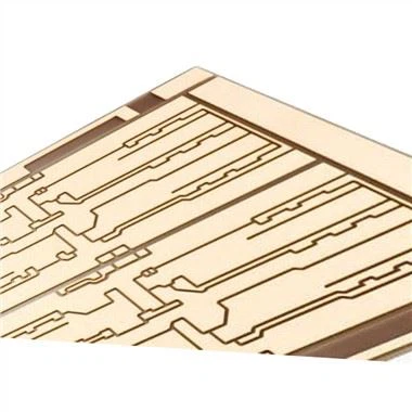
Multilayer Ceramic Substrate
Ceramic substrate refers to a special process board in which copper foil is directly bonded to the surface (single-sided or double-sided) of Al2O3 or AlN ceramic substrate at high temperature. Various patterns can be etched like a PCB board, and it has a large current-carrying capacity. Therefore, ceramic substrates have become the basic materials for high-power power electronic circuit structure technology and interconnection technology.
Description
Product Details
Name: Ceramic Substrate
Material: Ceramic
Board thickness: 1.6mm
Surface treatment: ENIG
Technology: Stack up N+N, Min Track/Width 3/3mil, Blind & Buried vias, laser vias
Payment: L/C,T/T,Western Union
Certification: UL Consumer (Wear, Electronic Digital, Household Appliances, Connectors)/Industrial Control/Automobile TS16949/Medical/Server, Cloud Computing & Base Station/Aviation/Military/Communication (Certification in Related Applications)
Delivery Term: DDU, FOB, CFA, CIF, CPT, EXW

What is the Ceramic Substrate
1. According to the material
(1) Al2O3
Alumina substrate is the most commonly used substrate material in the electronics industry, because it has high strength and chemical stability compared to most other oxide ceramics in terms of mechanical, thermal and electrical properties, and is rich in raw material sources, suitable for a variety of Technical manufacture as well as different shapes.
(2) BeO
It has a higher thermal conductivity than metal aluminum and is used in occasions where high thermal conductivity is required, but it decreases rapidly after the temperature exceeds 300 °C. The most important thing is that its toxicity limits its own development.
(3) AlN
AlN has two very important properties worth noting: a high thermal conductivity, and a matching expansion coefficient with Si. The disadvantage is that even a very thin oxide layer on the surface will have an impact on thermal conductivity, and only strict control of materials and processes can produce AlN substrates with better consistency. However, with the improvement of the economy and the upgrading of technology, this bottleneck will eventually disappear.
Based on the above reasons, it can be known that alumina ceramics are still widely used in the fields of microelectronics, power electronics, hybrid microelectronics, power modules and other fields due to their superior comprehensive performance.
2. According to the manufacturing process
At present, there are five common types of ceramic heat dissipation substrates: HTCC, LTCC, DBC, DPC, and LAM. Both HTCC and LTCC belong to the sintering process, and the cost will be higher.
However, DBC and DPC are domestically developed and mature technologies for energy production in recent years. DBC uses high-temperature heating to combine Al2O3 and Cu plates. The technical bottleneck is that it is difficult to solve the problem of micro pores between Al2O3 and Cu plates. , which makes the mass production energy and yield of this product greatly challenged, while DPC technology uses direct copper plating technology to deposit Cu on the Al2O3 substrate. The process combines materials and thin film technology. Its products are The most commonly used ceramic heat dissipation substrate in recent years. However, its material control and process technology integration capabilities are relatively high, which makes the technical threshold for entering the DPC industry and stable production relatively high. LAM technology is also known as laser rapid activation metallization technology.
(1) HTCC (High-Temperature Co-fired Ceramic)
HTCC is also known as high temperature co-fired multi-layer ceramics. The manufacturing process is very similar to LTCC. The main difference is that the ceramic powder of HTCC is not added with glass material. Therefore, HTCC must be dried and hardened at a high temperature of 1300~1600 °C. The green embryo is then drilled with via holes, and the holes and printed circuits are filled with screen printing technology. Due to the high co-firing temperature, the choice of metal conductor materials is limited. The main material is high melting point but conductive Metals such as tungsten, molybdenum, manganese...
(2) LTCC (Low-Temperature Co-fired Ceramic)
LTCC is also known as low temperature co-fired multi-layer ceramic substrate. In this technology, inorganic alumina powder and about 30%~50% glass material plus organic binder are firstly mixed to form a muddy slurry. Use a scraper to scrape the slurry into flakes, and then go through a drying process to form the flake slurry into thin green embryos, and then drill through holes according to the design of each layer, as the signal transmission of each layer, the internal circuit of LTCC Then, screen printing technology is used to fill holes and print circuits on the green embryo, respectively, and the inner and outer electrodes can be made of silver, copper, gold and other metals respectively. Sintering and molding in a sintering furnace can be completed.
(3) DBC (Direct Bonded Copper)
The direct copper coating technology is to directly bond copper on the ceramic by using the oxygen-containing eutectic liquid of copper. The basic principle is to introduce an appropriate amount of oxygen between the copper and the ceramic before or during the bonding process. In the range of ℃, copper and oxygen form a Cu-O eutectic liquid. DBC technology uses this eutectic liquid to chemically react with the ceramic substrate to generate CuAlO2 or CuAl2O4 phase, and on the other hand, infiltrate the copper foil to realize the combination of the ceramic substrate and the copper plate.

Superiority
◆The thermal expansion coefficient of the ceramic substrate is close to that of the silicon chip, which can save the Mo chip of the transition layer, save labor, material and cost;
◆Reduce solder layer, reduce thermal resistance, reduce voids, and improve yield;
◆Under the same current carrying capacity, the line width of 0.3mm thick copper foil is only 10% of that of ordinary printed circuit boards;
◆ Excellent thermal conductivity makes the package of the chip very compact, so that the power density is greatly improved, and the reliability of the system and device is improved;
◆ Ultra-thin (0.25mm) ceramic substrate can replace BeO, no environmental toxicity problem;
◆Large current carrying capacity, 100A current continuously passes through 1mm wide 0.3mm thick copper body, the temperature rise is about 17℃; 100A current continuously passes through 2mm wide 0.3mm thick copper body, the temperature rise is only about 5℃;
◆Low thermal resistance, the thermal resistance of 10×10mm ceramic substrate is 0.31K/W, the thermal resistance of 0.63mm thick ceramic substrate is 0.31K/W, the thermal resistance of 0.38mm thick ceramic substrate is 0.19K/W, and the thermal resistance of 0.25mm thick ceramic substrate Thermal resistance is 0.14K/W.
◆ High insulation withstand voltage to ensure personal safety and equipment protection.
◆ New packaging and assembly methods can be realized, so that the product is highly integrated and the volume is reduced.
Hot Tags: multilayer ceramic substrate, China, suppliers, manufacturers, factory, customized, buy, cheap, quotation, low price, free sample