What are the reasons for the copper exposure in the hot air leveling process of the PCB circuit board?
Jun 26, 2022
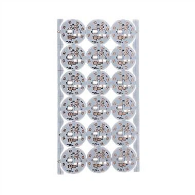
Hot air leveling is to immerse the printed circuit board in molten solder, and then use hot air to blow off the excess solder on its surface and metallized holes to obtain a smooth, uniform and bright solder coating with good solderability. The coating is completely free of exposed copper. The exposed copper on the surface of the pad and in the metallized hole after hot air leveling is an important defect in the inspection of the finished product, and it is one of the common reasons for the rework of the hot air leveling. So, what are the reasons for PCB hot air leveling to expose copper?

1. Insufficient pretreatment and poor roughening. The quality of the hot air leveling pre-treatment process has a great impact on the quality of the hot air leveling. This process must completely remove the oil, impurities and oxide layers on the pads to provide a fresh and solderable copper surface for tin immersion. The most commonly used pretreatment process is mechanical spraying. The phenomenon of exposed copper caused by poor pretreatment occurs in large quantities, and the exposed copper points are often distributed on the entire board surface, and it is more serious on the edge. In the event of a similar situation, chemical analysis of the micro-etching solution should be carried out, the second pickling solution should be checked, the concentration of the solution should be adjusted, and the solution that was seriously polluted due to long-term use should be replaced, and the spray system should be checked for smoothness. Properly extending the treatment time can also improve the treatment effect.
2. The surface of the pad is not clean, and there is residual solder resist contaminating the pad. Most manufacturers use full-board screen printing liquid photosensitive solder resist ink, and then remove excess solder resist through exposure and development to obtain a time-sensitive solder resist pattern. Whether there are defects on the solder mask film, whether the composition and temperature of the developer are correct, whether the speed of development, that is, whether the developing point is correct, etc., any of these conditions will leave residual spots on the pads. PCB design generally should set up a post to inspect the interior of the graphics and metallized holes before the curing process to ensure that the pads and metallized holes of the printed circuit board sent to the next process are clean and free of solder mask ink residues.
3. The flux activity is not enough. The role of the flux is to improve the wetting of the copper surface, protect the laminate surface from overheating, and provide protection for the solder coating. If the flux activity is not enough, the wettability of the copper surface is not good, and the solder cannot completely cover the pad, and the copper exposure phenomenon is similar to the poor pretreatment. Extending the pretreatment time can reduce the copper exposure phenomenon. The selection of a flux with stable and reliable quality by process technicians has an important influence on hot air leveling. Excellent flux is the guarantee of the quality of hot air leveling.