PCB Board Basic Knowledge
Feb 07, 2023
When making a robot, the PCB board is inevitable. The previous understanding of it will only be used at this level. Recently, I learned the production of PCB board and found that I did n’t know the knowledge before, so I sorted it out to share with you.
1. Pole from perforated-the connection channel of the double-layer board
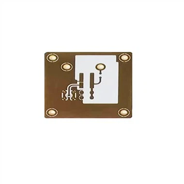
This is the most unpredictable link before. When you get a PCB, you will find that there are many small holes in the top of the needle. This is the over -hole. The structure is as follows.
Excessive holes
The effect of perforated is mainly to connect the copper wires on the front and back of the two plates. Most of the over -hole is the red area in the figure. When the front wire is staggered, it can be used. Just like "Interchange Bridge", the wiring of the two -dimensional plane is converted into a three -dimensional three -dimensional space. The excessive hole in the blue area is mainly to connect the copper plates on both sides to achieve the effect of "common ground".
2. pad-can actually be used to identify positive and negative electrodes
The pads are used for welding of component pins. The size is larger than over -holes. Interestingly, the pads are not only the shape of the round, but also the shape of the square. I didn't pay attention to this detail, haha)
There is also a small detail that some circular pads are cross -shaped, which directly ground the pin. The ground on thepcb board is actually connected to the negative pole. It is guaranteed that all GND pins are common.
3. Common electronic components
The most commonly used resistance will not be placed. Now the main use is the patch resistance, and there are few direct plug resistors.
The heart of the crystal-circuit board, the number above represents the frequency
Figure 3.1 Crystal
Capacitors, black cylindrical, flat shape
Digital tube, of course, now many direct displays are used directly
buzzer
Four-legged switch-pins with the same color in the figure.
4.PCB packaging
The so -called PCB packaging is to show the actual electronic component, chip and other parameters (such as components size and length, width and width, pipe spacing, etc.) in the form of pictures, so that they can be called when drawing the PCB diagram.
PCB is distinguished according to the installation method. It can be divided into patch devices, installation devices, special devices (sinking devices)
5. Silk print-Come on the name, right?
After designing a PCB, finally in the finished product, the logo of the studio, the satisfaction of the satisfaction. Of course, the main role of the silk printing is to indicate the corresponding component label .PCB design. You can use a piece of A4 paper. Print it down and put the components to see if there is a cover, whether the font size is suitable. The common logo is:
R (Resistance) resistance
U (UNIT) unit module/integrated circuit
C (CAPACITANCE) capacitance
Q three -level tube
X crystal
6. End language
Everyone who uses PCB should learn the production of PCB, including the design of the circuit, Altiumdesign/Protel, welding circuit board, etc. Maybe you never need to make a circuit board by yourself, but with these knowledge, you can make you faster Familiar with the circuit of the board and prepare for the writing program.