What is a blind buried via? What are the benefits of blind and buried vias in PCB design?
Nov 10, 2022
In PCB manufacturing, a topic that is often encountered is blind and buried vias. The advantages of blind and buried vias, how they are constructed, and why it is important to work with a professional PCB manufacturer who knows how to properly add blind and buried vias to a printed circuit board.
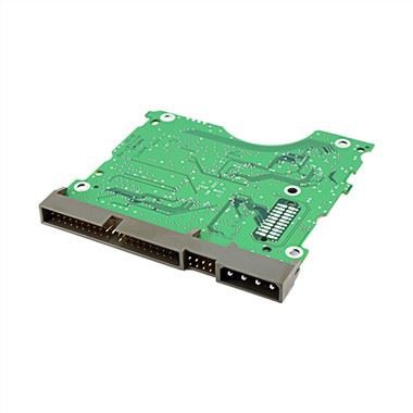
Under normal circumstances, it is difficult to mount all the links required on the PCB on one layer. The solution to this problem is vias. They are shaped like barrel-shaped conductive vias that allow for multilayer connections between circuit boards. Although there are more than one type of vias, two are the most commonly used. Both of these methods are blind vias and buried vias, which have certain benefits for those who use PCBs.
What is the difference between blind vias and buried vias? A blind via is one of the outer to inner layers that connects the board, however, it cannot exist all the time throughout the PCB. Vias connect inner layers without reaching outer layers. In addition, there is a via hole that runs vertically through the entire board and connects all the layers. This concept is relatively simple, understandable, and can also provide some advantages.
What are the benefits of blind and buried vias? Some PCB boards are designed to be small in size, and their space is limited. Therefore, blind and buried vias can provide more space and options for the plate. Buried vias, for example, will help free up space on the board without affecting surface devices or traces on the upper and lower layers. Blind holes help free up more space. They are often used on pitch BGA components. Because blind vias only pass through part of the thin plate, this also means that signal residue can be reduced.
Although blind vias and buried vias can be used on a wide variety of PCBs, they are typically used in high-density interconnect PCBs or HDIs. HDI can provide better power transfer and higher layer density. With hidden vias, this also helps make the board smaller and lighter, which is useful for making electronics. They are often used in medical equipment, computers, cell phones, and small electronics worn.
While blind and buried vias can help those in need, they also increase the cost of the PCB. This is because of the extra work required to add on the board and the required testing and fabrication. That said, use them only when you really need them; because you want a board that's both compact and efficient.
So how to build blind and buried vias? Vias can be formed before or after lamination of multiple layers. Blind vias and buried vias added to PCBs by drilling are very unstable. It is important that the builder knows and understands the depth of the drill bit. If the hole is not deep enough, there is no good connection. If the holes are too deep, they can degrade the quality of the signal or cause distortion. If these things had happened, it would have been impossible.
For blind holes, different drilling data are required to define the holes. The ratio of the diameter of the hole to the diameter of the drill should be equal to or less than that. The smaller the void, the smaller the distance between the outer layer and the inner layer.
When burying holes, a different drill file is required to make each hole. Because they are connected to different parts of the inner layer of the board. The ratio of hole depth to drill diameter should not exceed 12. If it is larger than this diameter, other connection plates may be touched.
It is recommended to make the PCB together with the advanced circuit. This will help ensure board design and construction, including blind and buried vias. Unpreparedness or inability to cooperate with a high-quality circuit board manufacturer can lead to increased costs, so be sure to find a professional fabricator. Professional tools and professional technicians are required to ensure proper drilling depth. Shenzhen Beton Co., Ltd. is a high-precision PCB multi-layer circuit board manufacturer, focusing on the production of PCB multi-layer boards, aluminum substrates, copper substrates, ceramic boards, high-frequency boards, FPC soft boards and rigid-flex boards, HDI high All kinds of special boards such as density interconnection board. During this process, ensure that the PCB is not exposed to the air, and the inner layers are properly coated and connected