


HDI 1+n+1 Circuit Board
HDI is a High Density Interconnector board, a printed circuit board manufactured by high density interconnection (HDI). The printed circuit board is a structural element formed by insulating materials supplemented by conductor wiring. When the printed circuit board is made into the final product, integrated circuits, transistors (transistors, diodes), passive components (such as resistors, capacitors, connectors, etc.) and various other electronic parts are mounted on it.
Description
Product Detail
As the electronics industry continues to change. Electronic products are developing towards lightness, thinness, shortness and miniaturization, and corresponding printed boards are also faced with the challenges of high precision, thin line and high density. The trend of circuit boards in the global market is to introduce blindness in high-density interconnect products. Buried vias can save time more effectively and make the line width and line spacing thinner and narrower.

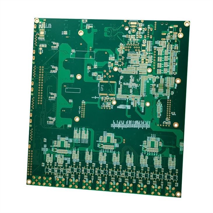
Layers: 8
Base Material:FR4 High Tg
Thickness:1.6±0.10mm
Min.Hole Size:0.15mm
Minimum Line Width/Space:0.10mm/0.10mm
Minimum Clearance between Inner Layer PTH and Line: 0.2mm
Size:225mm×168mm
Surface treatment:ENIG
Speciality: Laser via copper plated shut,VIPPO Technology,Buried Hole
Applications:Computer
The HDI N+n+N Type
1+N+1

In the 1+N+1 stacking type, "1" represents one sequential lamination on either side of the core. A continuous lamination adds two copper layers for a total of N+2 layers. The top layer has an additional laminate that allows holes to stack. This structure is suitable for BGAs with low input/output counts, and its installation stability is good.
2+N+2

Now, examine the 2+N+2 stack shown above. This structure contains 2 layers of high-density interconnects and is suitable for BGAs with smaller pitches and higher I/O counts. These designs use copper to fill staggered or stacked microvias, typically used in high-level signaling applications.
Any layer

Any layer structure is another approach used in HDI design. Any Layer PCB is the next level advancement in HDI PCB design, following the Class VI HDI standard. Any layer technology can be used for high-level interconnect applications, as all microvia layers are free to interconnect.
In this method, the microporous layers are used as redistribution layers in the prepreg, or they can be said to float in the prepreg. Microvias in a layer are first constructed following the process of drilling, filling, electroplating, printing, etching and lamination. Then, other layers are stacked on top of the existing layers after the same process.
Applications of HDI
While electronic design is constantly improving the performance of the whole machine, it is also trying to reduce its size. In small portable products from mobile phones to smart weapons, "small" is the eternal pursuit. High Density Integration (HDI) technology enables more miniaturization of end product designs while meeting higher standards for electronic performance and efficiency. HDI is widely used in mobile phones, digital (camera) cameras, notebook computers, automotive electronics and other digital products, among which mobile phones are the most widely used. HDI boards are generally manufactured by the build-up method. Ordinary HDI boards are basically one-time buildup, and high-end HDI uses two or more buildup technologies, while using advanced PCB technologies such as stacking, electroplating, and laser direct drilling. High-end HDI boards are mainly used in 5G mobile phones, advanced digital cameras, IC carrier boards, etc.
Beton FAQ
Q1. What is needed for quotation?
1.Gerber file & Bom list.
2.Clear pics of pcba or pcba sample for us.
3.Test method for PCBA.
Q2. Are my files safe?
Your files are held in complete safety and security. We protect the intellectual property for our customers are never shared with any third parties.
Q3.MOQ?
There is no MOQ. We are able to handle small as well as large volume production with flexibility.
Q4. Shipping cost?
The shipping cost is determined by the destination, weight, packing size of the products. Please let us know if you need us to quote you the freight.
Q5. How can you ensure the quality of the PCBs?
Our PCBs are 100% test including Flying Probe Test, E-test and AOI.
Hot Tags: hdi 1+n+1 circuit board, China, suppliers, manufacturers, factory, customized, buy, cheap, quotation, low price, free sample


