How to make pcb resin plugging
Jun 01, 2022
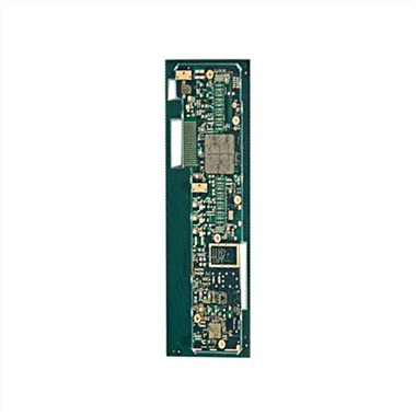
Pcb resin plugging is a widely used and favored process in recent years, especially for high-precision multilayer boards and products with larger thicknesses. Some problems that cannot be solved with green oil plug holes and press-fit resin are hoped to be solved by resin plug holes. Due to the characteristics of the resin itself, people still need to overcome many difficulties in the manufacture of the circuit board in order to make the quality of the resin plug hole better.

1. The production of the outer layer meets the requirements of the negative film, and the thickness-diameter ratio of the through hole is less than or equal to 6:1.
The conditions that need to be met for PCB negative film requirements are:
(1) Line width/line gap is large enough
(2) The maximum PTH hole is less than the maximum sealing ability of the dry film
(3) The thickness of the PCB is less than the maximum thickness required by the negative film, etc.
(4) Boards without special requirements, such as: partial electroplated gold board, electroplated nickel gold board, half-hole board, printed plug board, ringless PTH hole, board with PTH slot hole, etc.
Production of inner layer of PCB board → lamination → browning → laser drilling → debrowning → outer layer drilling → copper sinking → whole board hole filling and electroplating → slice analysis → outer layer pattern → outer layer acid etching → outer layer AOI →Follow-up normal process
2. The production of the outer layer meets the requirements of the negative film, and the thickness-diameter ratio of the through hole is more than 6:1.
Due to the thickness-to-diameter ratio of the through hole >6:1, the copper thickness requirement of the through-hole hole cannot be met by using the whole-board hole-filling electroplating. Copper plating to the required thickness, the specific operation process is as follows:
Production of inner layer → lamination → browning → laser drilling → debrowning → outer layer drilling → copper sinking → whole board hole filling and electroplating → full board electroplating → slice analysis → outer layer graphics → outer layer acid etching → follow-up Normal Process
3. The outer layer does not meet the negative film requirements, the line width/line gap ≥ a, and the outer layer through hole thickness-diameter ratio ≤ 6:1.
Fabrication of the inner layer of the circuit board → lamination → browning → laser drilling → debrowning → outer drilling → copper sinking → whole board filling and electroplating → slice analysis → outer layer pattern → pattern plating → outer layer alkaline etching →Outer AOI→Follow-up normal process
Four: The outer layer does not meet the requirements of the negative film, the line width/line gap <a; or the line width/line gap ≥ a, the thickness-diameter ratio of the through hole> 6:1.
Fabrication of inner layer → pressing → browning → laser drilling → debrowning → copper sinking → whole board hole filling and electroplating → slice analysis → copper reduction → outer layer drilling → copper sinking → full board plating → outer layer graphics → Pattern electroplating→outer layer alkaline etching→outer layer AOI→subsequent normal process
Pcb resin plug hole production process: first drill, then plate the hole through, then plug the resin for baking, and finally grind (smooth). The polished resin does not contain copper, and a layer of copper needs to be added to turn it into PAD. This step is done before the original PCB drilling process. First, the holes of the fortress holes are processed, and then drilled. For other holes, follow the original normal process.

Knowledge expansion:
When the plug hole is not plugged well and there are air bubbles in the hole, the air bubbles are likely to explode when the PCB board passes through the tin furnace because it is easy to absorb moisture. In the production process of the pcb resin plug hole, if there are air bubbles in the hole, these air bubbles will be discharged by the resin during baking, resulting in a situation where one side is concave and one side is protruding. We can directly detect this defective product. Of course, if the PCB board that just leaves the factory has been baked when it is loaded, there will be no explosion of the board in general.