
Professional Blood Pressure Meter PCB and PCBA Manufacturer
Alumina substrate is the most commonly used substrate material in the electronics industry, so the ceramic board will be made of alumina substrate material to make Alumina multilayer Board Ceramic PCB. Because of its high strength and chemical stability, and rich raw materials. So it is suitable for various technical manufactures and different shapes.
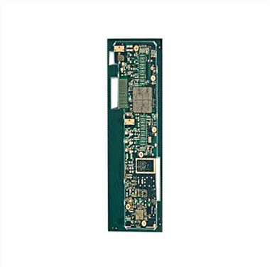
Description
Our company adheres to the development strategy of internal management and external market, and wholeheartedly creates the latest and best new Electronic Components Sourcing Service, Multilayer PCB Printed Circuit Board Prototype, Fr4 PCB Electronic Components for the majority of new and old customers and provides the most satisfactory service. We look forward to integrating internal and external resources in various ways such as capital operation and business cooperation, and ramming to build a client-oriented and business management platform. We sincerely welcome clients from both of those at your home and overseas to occur to barter business enterprise with us. We do things with enthusiasm, ability and vitality.
Product Detail
Material :Alumina ceramic ( Al2O3 ) Ceramic thickness : 1.0 mm Conductor: Silver Silver Thickness: 20 um Special: Resistor Other : DIP solder connector Application :High voltage Power supply |  |
Now Ceramic PCB has been widely used because of its high thermal conductivity, low CTE, low dielectric constant and chemical erosion resistance.

With the development of chip components and surface mount technology (SMT) in electronics industry, traditional printed circuit boards with organic laminates as based material are developing towards high density, high precision, and high reliability.
Ceramic PCB Types According to PCB Manufacturing Process:
High Temperature Co-fired Ceramic (HTCC) PCB:
The main components of HTCC ceramic substrates are alumina, plasticizers, binders, lubricants and solvents. This mixture will form a green ceramic, which is then calendered and curtain coated. Tungsten or molybdenum can be used as the metal for circuit printing. Next, it is exposed to a high temperature of 1700 OC and baked in hydrogen for 32 to 48 hours. It is then laminated and cut. This is suitable for small size ceramic boards and not for large size ceramic boards due to inappropriate shrinkage tolerances and poor warpage
Low Temperature Co-fired Ceramic (LTCC) PCB:
This is a combination of glass crystals and glass composites. In addition, other ingredients such as binders and non-glass ingredients are added. Then, circuit traces are created using a highly conductive gold paste, which is then treated/baked in an oxidizing gas furnace at 900 OC.
Thick Film Ceramic PCB:
Here, two alternating thick films are applied on a ceramic substrate. One is gold thick film and the other is dielectric thick film, but since gold is expensive, copper thick film is implemented, which is a recognized technology for ceramic PCBs. The stack is then moved into a filled bake oven (copper to avoid oxidation), in which it is processed in nitrogen at a temperature of 1000 Ó C. The dielectric paste is produced from nitrogen.
Application of ceramic PCB:
1- High current bright LED lights and spotlights.
2- Automotive electronics such as power controllers, optical systems, power converters and power conditioners
3- Industrial power equipment such as servo drives, robots, etc.
4- Microprocessor, Graphics Card and IC Array
5- Semiconductor Devices
6- Audio Power Amplifier Based on High Power Transistor
7-Solar battery related circuits, inverters, chargers, etc.
8- DC-DC regulators and power management circuits, etc.
FAQs
Q1: What’s the Aluminum board Thermal Conductivity?
Reply: Usually use 0.8-3W/m.K. If you have special demands, such as COB(chip on board) please feel free contact us.
Q2: Is my PCB Gerber file safe if I send it to you for manufacturing?
Reply: We respect customer’s design authority and will never manufacture PCB for someone else without your permission. NDA is acceptable.
Q3:What is your testing policy and how you control the quality?
Reply: For sample, usually tested by flying probe; for PCB volume over 3 square meters, usually tested by fixture, this will be more faster. E-test will be charged only one time. If flying probe test chosen, such test cost will be recharged for any repeat orders.
Q4: What files should we offer?
Reply: If only need PCB, please provide Gerber File and manufacturing specifications; If need PCBA,Please provide Gerber File, Manufacturing specification, BOM list and Pick & Place/XY file.If you don’t have PCB Gerber file, you can send us the PCB sample and tell us the requirement, we can make it.
Q5: How to contact us?
Reply: You can contact us online, telephone, skype, email, and Whatsapp, Wechat and so on. We will reply to you in time within half an hour.
Since the establishment of the company, through continuous technological innovation, the product manufacturing process has been improved day by day, the production scale has been continuously improved, and it has developed into a large-scale Professional Blood Pressure Meter PCB and PCBA Manufacturer production enterprise in China. We deeply realize that innovation is the inexhaustible driving force and advantage of our company's development. With the eternal goal of 'continuous quality improvement, customer satisfaction', we are sure that our product quality is stable and reliable and our products are best-selling at home and abroad.
Hot Tags: alumina multilayer board ceramic PCB, China, suppliers, manufacturers, factory, customized, buy, cheap, quotation, low price, free sample, Double Sided Prototype Flexible Circuit PCB Board, Ceramic Pcb With Ain Base Material, Automotive PCB Assembly, Fine Quality 2f Communication Composite Board, Oem Air Conditioner Control Circuit PCB Board, Doubled-sides Rigid-flex PCB
Send Inquiry
You Might Also Like
-

Hot Sale Industrial Control Panel PCB HDI PCB Circui...
-

Professional Flexible Circuit Board FPC for LED Stri...
-
Side Emitting Flexible LED Strip PCB Board FPC Light...
-
6layer 1.0mm Thickness Enig, Min. Pad 4mil PCB Fabri...
-

PCBA Board Assembly for Automotive and Industial Con...
-

LED Light PCB Assembly White Solder Mask