
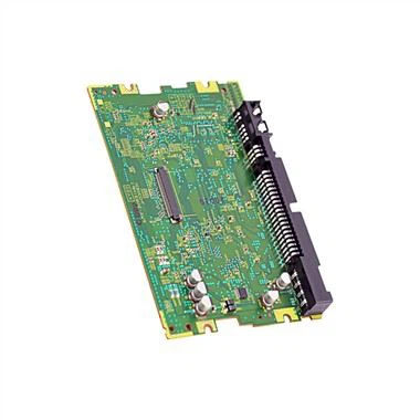
Corrosion Resistance Precision Thick Film Printed Multilayer Alumina Ceramic Circuits ...
Alumina substrate is the most commonly used substrate material in the electronics industry, so the ceramic board will be made of alumina substrate material to make Alumina multilayer Board Ceramic PCB. Because of its high strength and chemical stability, and rich raw materials. So it is suitable for various technical manufactures and different shapes.
Description
With quite a few factories, we can easily provide a wide vary of Industrial Control PCB Assembly, Electronic Components Sourcing Service, Double Panel Golden Finger Pcb. Integrity means that we treat our employees, customers, suppliers, government, society, shareholders, partners and other related parties with sincerity, and are committed to establishing long-term win-win relationships with all related parties. Our past is accompanied by a series of conceptual innovation, institutional innovation, management innovation and technological innovation.
Product Detail
Material :Alumina ceramic ( Al2O3 ) Ceramic thickness : 1.0 mm Conductor: Silver Silver Thickness: 20 um Special: Resistor Other : DIP solder connector Application :High voltage Power supply |  |
Now Ceramic PCB has been widely used because of its high thermal conductivity, low CTE, low dielectric constant and chemical erosion resistance.

With the development of chip components and surface mount technology (SMT) in electronics industry, traditional printed circuit boards with organic laminates as based material are developing towards high density, high precision, and high reliability.
Ceramic PCB Types According to PCB Manufacturing Process:
High Temperature Co-fired Ceramic (HTCC) PCB:
The main components of HTCC ceramic substrates are alumina, plasticizers, binders, lubricants and solvents. This mixture will form a green ceramic, which is then calendered and curtain coated. Tungsten or molybdenum can be used as the metal for circuit printing. Next, it is exposed to a high temperature of 1700 OC and baked in hydrogen for 32 to 48 hours. It is then laminated and cut. This is suitable for small size ceramic boards and not for large size ceramic boards due to inappropriate shrinkage tolerances and poor warpage
Low Temperature Co-fired Ceramic (LTCC) PCB:
This is a combination of glass crystals and glass composites. In addition, other ingredients such as binders and non-glass ingredients are added. Then, circuit traces are created using a highly conductive gold paste, which is then treated/baked in an oxidizing gas furnace at 900 OC.
Thick Film Ceramic PCB:
Here, two alternating thick films are applied on a ceramic substrate. One is gold thick film and the other is dielectric thick film, but since gold is expensive, copper thick film is implemented, which is a recognized technology for ceramic PCBs. The stack is then moved into a filled bake oven (copper to avoid oxidation), in which it is processed in nitrogen at a temperature of 1000 Ó C. The dielectric paste is produced from nitrogen.
Application of ceramic PCB:
1- High current bright LED lights and spotlights.
2- Automotive electronics such as power controllers, optical systems, power converters and power conditioners
3- Industrial power equipment such as servo drives, robots, etc.
4- Microprocessor, Graphics Card and IC Array
5- Semiconductor Devices
6- Audio Power Amplifier Based on High Power Transistor
7-Solar battery related circuits, inverters, chargers, etc.
8- DC-DC regulators and power management circuits, etc.
FAQs
Q1: What’s the Aluminum board Thermal Conductivity?
Reply: Usually use 0.8-3W/m.K. If you have special demands, such as COB(chip on board) please feel free contact us.
Q2: Is my PCB Gerber file safe if I send it to you for manufacturing?
Reply: We respect customer’s design authority and will never manufacture PCB for someone else without your permission. NDA is acceptable.
Q3:What is your testing policy and how you control the quality?
Reply: For sample, usually tested by flying probe; for PCB volume over 3 square meters, usually tested by fixture, this will be more faster. E-test will be charged only one time. If flying probe test chosen, such test cost will be recharged for any repeat orders.
Q4: What files should we offer?
Reply: If only need PCB, please provide Gerber File and manufacturing specifications; If need PCBA,Please provide Gerber File, Manufacturing specification, BOM list and Pick & Place/XY file.If you don’t have PCB Gerber file, you can send us the PCB sample and tell us the requirement, we can make it.
Q5: How to contact us?
Reply: You can contact us online, telephone, skype, email, and Whatsapp, Wechat and so on. We will reply to you in time within half an hour.
With advanced technology, excellent quality and satisfactory service concept, wer will lead the industry of Corrosion Resistance Precision Thick Film Printed Multilayer Alumina Ceramic Circuits ... to a higher level, can develop and make products for your special purpose. Warmly welcome your visiting and hope we can work with you in the future. Our products are mature, deeply loved by the majority of users, our market demand is huge, the prospect is broad. We always take integrity as the foundation and innovation as the driving force for development.
Hot Tags: alumina multilayer board ceramic PCB, China, suppliers, manufacturers, factory, customized, buy, cheap, quotation, low price, free sample, Smart Home PCB Assembly, High Tg FR4 HDI PCB, Industrial Control PCB Assembly, 12v Emergency Light Circuit Board Assembly, Doubled Sides PCB Fabrication and Assembly, Multilayer Board FPC Circuit Board
Send Inquiry
You Might Also Like
-

Dihong Multilayer PCB Circuit Boards Design Printed ...
-

SMT Reflow Soldering Machine for PCB Soldering
-
Custom Double-Sided Flex Strip PCB and FPC Board
-

ODM Fr4 SMT Electronic PCB Assembly PCBA
-
Hotselling Micro Flow Peristaltic Infusion Pump Powe...
-

PCB Board LED Factory and Circuit Board PCB with PCB...