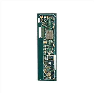
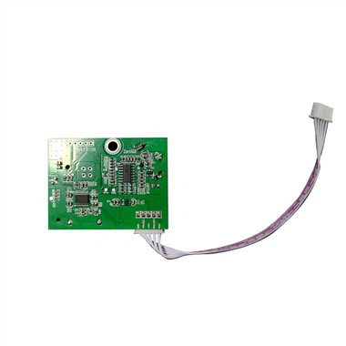
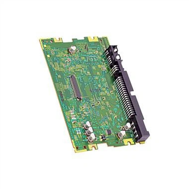
Robotic Car PCB Assembly
SMT patch refers to the abbreviation of a series of technological processes that are processed on the basis of PCB. We can manufacture robotic car PCB assembly. SMT is the most popular technology and process in the electronic assembly industry.
Description
Product Detail
Robotic car PCB assembly | |
Layers:2 Layer Base Material:FR-4 Copper Thickness:1oz Board Thickness:1.6mm Min. Hole Size:4mil Min. Line Width:4mil Min. Line Spacing:4mil Surface Finish: HASL Lead Free PCBA Test:100% Function Testing | Dimension Tolerance:±0.13mm Minimum line width:0.1mm Minimum Line Space:0.1mm
DK Thickness:0.076 to 6.00mm
Board Thickness Tolerance:±10%
Laser drill hole size:0.1mm
PCB Test:100% Testing
Maximum Dimension:610 x 1100mm
Solder Mask Color: Green, Yellow, Black, Purple, Blue, White and Red
|

The automotive electronics market is the third largest application area of PCB after computers and communications. With the gradual evolution and development of automobiles from mechanical products in the traditional sense into high-tech products of intelligence, informatization and mechatronics, electronic technology has been widely used in automobiles, whether it is engine system, chassis system, Electronic products are used in safety systems, information systems, and in-vehicle environment systems without exception. The automotive market has obviously become another bright spot in the consumer electronics market. The development of automotive electronics has naturally driven the development of automotive PCBs.
Among the key application objects of PCB today, automotive PCB occupies an important position. However, due to the special working environment, safety and high current requirements of automobiles, it has higher requirements on PCB reliability and environmental adaptability

The bottom of the PCB consists of several layers like this.
⑴Substrates: These are specialized materials that conduct electricity minimally. Common substrates used as insulating layers between two conductive copper layers are fluorine series resins, PPO or PPE resins and modified epoxy resins, fluorine series dielectric substrates, PTFE, etc.
⑵ Copper: A thin layer of copper foil is added to improve the thermal resistance and current carrying capacity of the PCB.
⑶Solder resist: usually green solder resist, used to insulate copper wires from other conductive materials.
⑷ Silkscreen: The final layer silkscreen of the PCB, which helps provide text indicators for the part. Silkscreen layers help identify test points, part numbers, warning symbols, logos and manufacturer markings.
The basic layers above are pretty much the same for all types of PCBs. The only thing that differs on rigid, flex, metal core, surface mount or through hole PCBs is the use of a substrate. The manufacturer chooses the substrate after considering the application.
SMD process
One-sided assembly
Incoming inspection => silk screen solder paste (spot glue) => patch => drying (curing) => reflow soldering => cleaning => inspection => rework
Double-sided assembly
A: Incoming material inspection => PCB's A side silk screen solder paste (spot glue) => SMD PCB B side silk screen paste (spot glue) => SMD => drying => reflow soldering ( It is better to only do the B side => cleaning => inspection => rework).
B: Incoming material inspection => PCB's A-side screen printing solder paste (spot adhesive) => SMD => drying (curing) => A-side reflow soldering => cleaning => flip = PCB's B-side point SMT glue => SMD => curing => B-side wave soldering => cleaning => inspection => repair)
This process is suitable for reflow soldering on the A side of the PCB and wave soldering on the B side. In the SMD assembled on the B side of the PCB, this process should be used when only the SOT or SOIC (28) pins are below.
Hot Tags: robotic car pcb assembly, China, suppliers, manufacturers, factory, customized, buy, cheap, quotation, low price, free sample