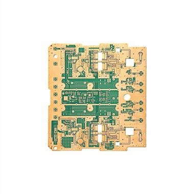
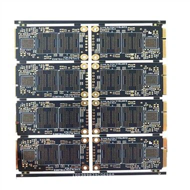
How Pcbs Are Manufactured
Oct 28, 2022
PCB fabrication involves converting design files, including Gerbers and netlists, into physical circuit boards on which components can be placed and soldered.
The manufacturing process begins with design output files (Gerbers, netlists, drill files, etc.). These output files are generated during the design phase, including developing product concepts, schematic input, layout design, and file generation. The next stage includes the fabrication and assembly of the circuit boards.
The flowchart below shows the steps involved in PCB fabrication.

A. Design and Board Output Files
After receiving the design files from the PCB designer, manufacturing begins quickly. Designers create output files in Gerber or ODB++ format for manufacturing and create bills of materials (BOMs) for assembly.

Manufacturers perform DFM inspections to identify potential risks and errors that may arise in the manufacturing process. Designers/clients are alerted if anything goes wrong. The corrected file is then fed into a CAM (Computer Aided Manufacturing) system to recognize the format of the artwork layers, drill hole data, IPC netlist, and convert the electronic data into an image. It also verifies layer order, runs Design Rule Checks (DRC), and does many other things.
All layers are analyzed using a Gerber file as input. The stacking plan will also proceed accordingly. Later, CAM will create output files for the various manufacturing departments. Output files include drill programs (sub and main drill holes), imaging layers, solder mask file output, routing files, and IPC netlists.

B. Inner Layer Imaging
Manufacturers mostly use LDI (Laser Direct Imaging) due to miniaturization. They also used a special printer called a plotter, which made photographic films of circuit layers, solder mask and silkscreen layers to print circuit images. The panel consists of a photosensitive film called photoresist. Photoresists include a layer of photoreactive chemicals that polymerize upon exposure to ultraviolet light. The panel is now under a computer-controlled laser. The computer scans the surface of the circuit board and converts it into a digital image. This digital image is matched to a preloaded CAD/CAM design file containing the required image specifications. In the same way, a negative image is formed on the inner layer.

The process flow of LDI is shown in the following figure:

After developing the image, the unhardened photoresist (the copper needed for protection) is removed with an alkaline solution.
C. Etching
In PCB manufacturing, etching is the process of removing unwanted copper (Cu) from the board. Unwanted copper is nothing but non-circuit copper. As a result, a desired circuit pattern is obtained.
Circuit board manufacturers typically use wet etching processes. In wet etching, unwanted materials dissolve when immersed in chemical solutions.

Important parameters to consider during the etching process are the speed at which the panel is moved, the spray of chemicals, and the amount of copper to be etched away. The entire process is carried out in a conveyor-type high-pressure atomizing chamber.
D. Photoresist Stripping
During this process, the remaining photoresist is etched away from the copper. The process involves using a high pressure water rinse to dissolve corrosive particles (chemical agents) in the water, which destroy the photoresist.
E. Punch after inspection and etching
With all layers clean and ready, the manufacturer makes sure to punch alignment holes using the targets provided on the inner layers for better layer-to-layer alignment. The layers are placed in an optical punch to achieve precise inner and outer layer alignment.
Inspection in this method is accomplished by visually scanning the surface of the circuit board. The circuit board is illuminated by various light sources, for which one or more high-definition cameras are used. This is how an AOI (Automated Optical Inspection) system builds a complete image of the board for verification.
F. Brown oxide coating
Here, the copper circuit pattern is coated with brown oxide to prevent oxidation and corrosion of the inner layers after lamination. Additionally, it provides better bonding properties for bonding with prepregs.
G. Lamination
Lamination is the process of bonding prepreg, copper foil, inner core in a symmetrical stack under controlled temperature and pressure. It's a two-step process:
Stackup preparation
Bonding
Multilayer boards are made of copper foil, prepreg and inner core. These are held together by applying heat and pressure. For better bonding, mechanical presses are used for both hot and cold pressing. The bonder computer manages the process of heating the stack, applying pressure, and allowing the stack to cool at a controlled rate.

The following diagram summarizes the LDI process:

H. Drilling
During the drilling process, drill holes for through holes and lead components. The X-ray drill locates the target in the inner layer. The machine precisely drills the pilot holes. The machine is computer controlled, where the operator can select a specific drilling program. It positions the XY coordinates in the correct direction. Holes up to 100 microns in diameter can be drilled. The machine can also select the correct size drill and perform accordingly.

Drilling holes creates raised ends of metal commonly called burrs. The deburring process removes any burrs or impurities from the surface of the circuit board.

1. Electroless copper plating
The first step in the electroplating process is to make the hole barrel conductive by chemically depositing a very thin layer of copper on the hole walls. This process is called electroless copper plating. The reaction is initiated by a catalyst. After thorough cleaning, the panels go through a continuous chemical bath. A layer of copper about 0.08 to 0.1 microns thick is deposited on the hole barrel and on the surface of the panel.

J. Outer Layer Imaging
We use photoresist on the panel for inner layer imaging. Similarly, the outer layer of the panel will be imaged using a positive image. Here, the process follows the printing plate etching method. The first step involves cleaning the panel to prevent contamination and dust particles from adhering to the panel. Next, a layer of photoresist is applied to the panel. After this, LDI is used to print the image.
K. Copper Plating
In this step, the holes and surfaces are electroplated with copper. The panel is loaded into the flight stick by the operator. The panel acts as a cathode for electroplating the holes and surfaces, as the holes have deposited a thin layer of conductive copper, ready for electroplating. It is done by automatic plating line. Before electroplating, the panels are cleaned and activated in multiple baths. Each set of panels is computer controlled to ensure they stay in each tub for a precise specific amount of time. Typically, 1 mil thick copper is deposited in the hole barrel.

After copper plating, tin plating is next. Tin plating is used as a resist. It prevents corrosion of surface features such as copper pads, hole pads and hole walls during outer layer etching.

L. Photoresist Stripping
Once the panel is plated, the photoresist becomes undesirable and needs to be stripped from the panel to expose the unwanted copper. Here, a continuous line is used to dissolve and wash away the resist covering the unwanted copper. This is the first stage of the lift-etch-stripping process.

M. Final Etch
In this step, the unwanted exposed copper is removed using an ammonia etchant. At the same time, tin can hold the desired copper. At this point, the conductive areas and connections are properly established.

N. Tin stripping
After etching, the tin layer on the copper traces will be removed. Concentrated nitric acid is used to remove the tin, it won't damage the copper circuit tracks below it. This results in clear, distinct copper traces on the PCB.

O. Solder mask application
Solder mask has the following uses:
It provides insulation resistance for traces.
Distinguish weldable and non-weldable areas.
Provides protection from environmental conditions by covering non-weldable areas with ink.
LPI (Liquid Photo Imaging) masks combine solvents with polymers to form a thin coating that adheres to different circuit board surfaces. The printer images the coated panel. The UV light in the machine hardens the ink in the clear areas. After that, strip all unhardened resist from the imaging panel.
LPI curing (drying) combines the ink with the dielectric. It facilitates solder mask adhesion. The final baking step takes place in an oven or under an infrared heat source.

Green was chosen as a typical solder mask color because it does not strain the eyes. Before machines can inspect PCBs during production and assembly, all inspections are done manually. The overhead lights that technicians use to inspect circuit boards are not reflected by the green solder mask, making them safer for their eyes.
P. Surface finish
PCB finish is the metal-to-metal connection between bare copper and components on the solderable area of the circuit board. The substrate copper surface of a circuit board is susceptible to oxidation without a protective coating. Therefore, surface finish application is critical to protect it from oxidation. Additionally, it prepares components for soldering to the board during assembly and extends the shelf life of the board.
There are various types of surface treatments. However, lead-free surface finishes are widely used due to strict RoHS specifications.

Factors such as cost, environment, component selection, shelf life and yield should be considered when choosing a finish.

Q. Silkscreen
In this process, an inkjet projector is used to image the legend directly from the digital data of the circuit board. The ink is screen printed (smeared) on the surface of the panel using an inkjet printer. The panel is then baked to cure the ink. It specifies different types of text such as part numbers, names, codes, logos, etc.
There are three printing methods:
Manual screen printing
Direct legend printing

R. Electrical Test
E-test stands for bare printed circuit board electrical test. In this step, use an electronic probe to check each unmounted circuit board for shorts, opens, resistance, capacitance, and other basic electrical characteristics. E-test checks the conductivity of the board against the netlist file. The netlist contains information about the conductive interconnection patterns of the PCB.
Implement bed of nails and flying probe testing to test functionality.

Flying probe test
Flying probe testing uses a probe that moves from one point to another according to instructions provided by specific software. This is a fixtureless testing method. At the beginning, a flying probe test program (FPT) is generated and then loaded into the FPT tester. The tester applies electrical signals and power to the probe points, which are then measured according to the test procedure.
Bed of nails
The bed of nails is the traditional method for electrical testing of bare boards. It requires creating a test template with pins aligned with test locations on the PCB. The process is fast and suitable for large-scale production systems.
S. Analysis and v-scoring
The circuit boards are shaped and cut from the production panels in the final manufacturing stage. The method used is either to use a post hole or a V-shaped slot. V-grooves cut diagonal channels on both sides of the board, while postholes leave side grooves along the border. In any case, the boards can simply be ejected from the panel.