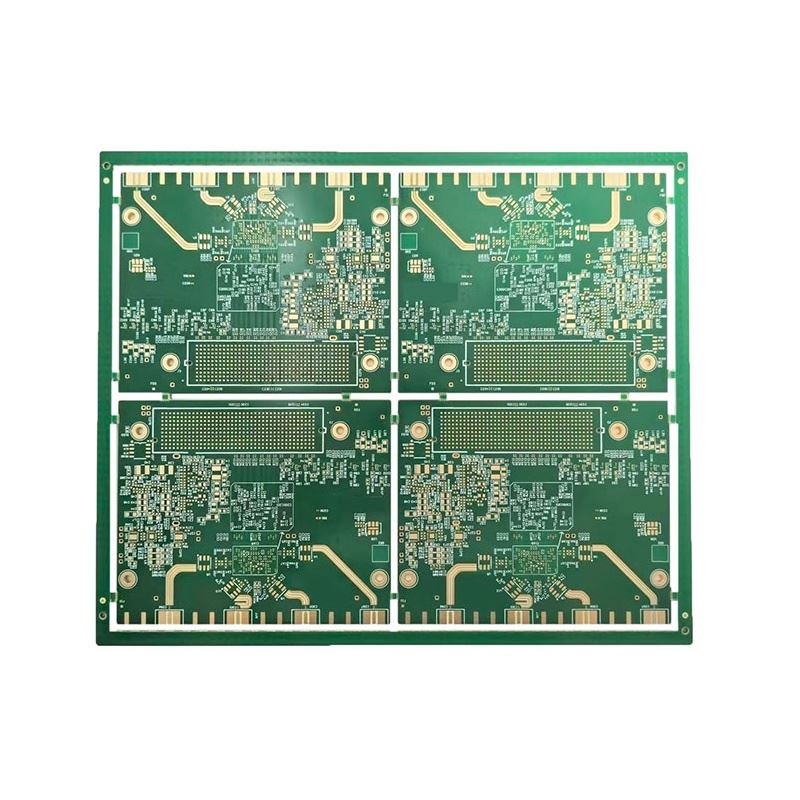

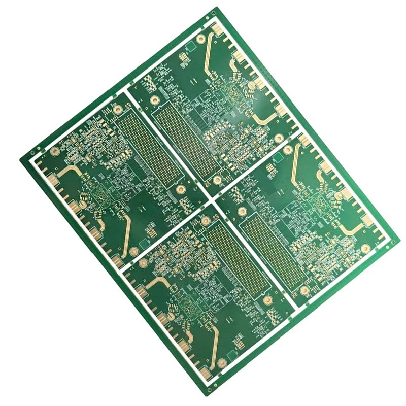
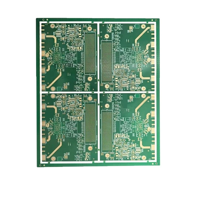
High-Precision 14-Layer HDI PCB: ENEPIG Finish & IPC Class 3 Reliability
This premium 14-layer High-Density Interconnect (HDI) printed circuit board is engineered for mission-critical applications where durability and signal integrity are paramount. Manufactured to strict IPC Class 3 standards, this board is ideal for aerospace, medical, and high-end industrial sectors that demand zero-failure performance.
Description
Technical Specifications
Layer Count: 14 Layers
Manufacturing Standard: IPC Class 3 Compliant (IAW IPC-6012 & IPC-A-600)
Surface Finish: ENEPIG (Electroless Nickel Electroless Palladium Immersion Gold)
Via Technology: Blind Vias (L1-L2, L13-L14) and Thru Vias (L1-L14)
Via-in-Pad Process: IPC-4761 Type VII (Non-conductive fill & capped)
Material: High-TG FR4 (IAW IPC-4101B/24, 26, or 28)
Plating Specs: Min. average 0.025mm copper in PTH
Edge Plating: Selective plating on designated mechanical layers for EMI shielding
Panelization: 4-up array with V-CUT (Scoring) for automatic SMD assembly
Core Manufacturing Strengths
1. IPC Class 3 Reliability & "No-Repair" Policy
In accordance with IPC Class 3 requirements for high-performance electronics, we strictly enforce a Zero-Repair policy. Any board that does not meet the initial fabrication criteria is rejected to ensure maximum field reliability. We provide a full IPC Class 3 Compatibility Report with every delivery.
2. Advanced Via-in-Pad (IPC-4761 Type VII)
Our facility utilizes state-of-the-art non-conductive via filling and metallized capping. This process ensures a perfectly flat pad surface, which is critical for high-density BGA mounting and superior thermal management.
3. Complex Blind Via Management
Our engineering team is expert at managing intricate drill pairs as defined in .GD1, .GD2, and .GD3 layers. We ensure precise registration (within .002 inch) for:
L1-L2 Blind Vias
L13-L14 Blind Vias
Full Stack Thru-vias
4. Specialized Edge Plating
We offer precision Edge Plating on specific sections (as per .GM3 layer) while maintaining strict clearances for center conductors and gap areas. This provides optimal grounding and EMI protection for sensitive high-frequency designs.
Engineering Consultant Services (DFM Support)
We go beyond simple fabrication. For high-layer counts, we provide professional DFM (Design for Manufacturing) advice, including:
Bond Enhancement Treatment: Optimization of chemical/mechanical treatments to maximize interlayer adhesion.
Foil Profile Selection: Expert guidance on selecting the right copper foil profile to balance signal integrity (Low-loss) and peel strength.
Quality Assurance & Compliance
100% Netlist Testing: Applied IAW IPC-9252 to ensure circuit continuity.
Solderability: Guaranteed IAW J-STD-003, Class 3, Category 2.
Flatness Control: Maximum allowable warpage and twist is strictly limited to 0.75% or less.
Traceability: Full Certificate of Compliance (CoC) provided.
Target Applications
Aerospace & Defense: Flight control systems and avionics.
Medical Technology: Life-support systems and high-resolution imaging.
Telecommunications: High-speed routers and switching equipment.
Industrial Automation: Precision robotics and control modules.
Contact Our Engineering Team
Ready to discuss your 14-layer project? Send your Gerber files and stack-up requirements to us. We provide comprehensive DFM reviews within 24 hours.
[Request a Quote for IPC Class 3 PCB]
Hot Tags: high-precision 14-layer hdi pcb: enepig finish & ipc class 3 reliability, China, suppliers, manufacturers, factory, customized, buy, cheap, quotation, low price, free sample