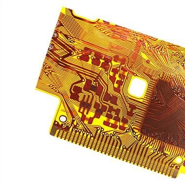
Ultra Thin Flexible PCB
Ultra thin flexible pcb is high wiring density, light weight, thin thickness and good bendability. Any FPC demands, please feel free to contact us.
Description
Product details
Ultra thin flexible pcb capability:
Base material: FR4 Tg 130, Tg 150, Tg 170, Tg 180, and BT material.
Board Thickness: 0.076~0.3 mm
Copper thickness: 0.5 OZ, 1 OZ, 2 OZ, 3 OZ
Outline: Routing, punching, V-Cut, laser cutting
Solder mask: Bare/White/Black/Blue/Green/Red Oil
Legend/Silkscreen Color: Black/White
Surface finishing: Immersion Gold, OSP, ENEPIG, HAL-LF (not popular)
Max Panel size: 500*650 mm , or 1200*450 mm
Min Panel size: 25*25 mm
Min single size: 3.0*3.0 mm
Min vias: 0.1 mm
Min traces space/width: 2.2mil/2.2mil
Packing: Vacuum
Samples L/T: 3~4 Days
Batch order L/T: 8~10 Days

Features of flexible circuit boards
⒈Short: The assembly time is short, all the lines are configured, and the connection work of redundant cables is omitted;
⒉Small: The volume is smaller than rigid PCB, which can effectively reduce the product volume and increase the convenience of carrying;
⒊Light: lighter weight than rigid PCB can reduce the weight of the final product;
4. Thin: The thickness is thinner than rigid PCB, which can improve the softness and strengthen the assembly of three-dimensional space in a limited space.
Common substrate material types for flexible PCBs

(1)Matrix:
The most important material in a flexible PCB or rigid PCB is its base substrate material. It is the material on which the entire PCB stands. In rigid PCBs, the substrate material is usually FR-4. However, in Flex PCB, the commonly used substrate materials are polyimide (PI) film and PET (polyester) film, in addition to this, polymer films such as PEN (polyethylene phthalate) can also be used Diester), PTFE and Aramid etc.
Polyimide (PI) "thermoset resins" are still the most commonly used materials for Flex PCBs. It has excellent tensile strength, is very stable over a wide operating temperature range of -200 OC to 300 OC, chemical resistance, excellent electrical properties, high durability and excellent heat resistance. Unlike other thermoset resins, it retains its elasticity even after thermal polymerization. However, PI resins have the disadvantage of poor tear strength and high moisture absorption. PET (polyester) resins, on the other hand, have poor heat resistance, "making them unsuitable for direct soldering", but have good electrical and mechanical properties. Another substrate, PEN, has intermediate-level performance better than PET, but not better than PI.
(2)Liquid Crystal Polymer (LCP) Substrates:
LCP is a rapidly popular substrate material in Flex PCBs. This is because it overcomes the shortcomings of PI substrates while maintaining all the properties of PI. LCP has 0.04% moisture and moisture resistance and a dielectric constant of 2.85 at 1 GHz. This makes it famous in high-speed digital circuits and high-frequency RF circuits. The molten form of LCP, called TLCP, can be injection molded and pressed into flexible PCB substrates and can be easily recycled.
(3)Resin:
Another material is the resin that tightly bonds the copper foil and base material together. The resin can be PI resin, PET resin, modified epoxy resin and acrylic resin. The resin, copper foil (top and bottom) and substrate form a sandwich called a "laminate". This laminate, called FCCL (Flexible Copper Clad Laminate), is formed by applying high temperature and pressure to the "stack" through automated pressing in a controlled environment. Among these mentioned resin types, modified epoxy resins and acrylic resins have strong adhesive properties.
So the solution to this problem is to use a 2-layer FCCL without adhesive. 2L FCCL has good electrical properties, high heat resistance and good dimensional stability, but its fabrication is difficult and expensive.
(4)Copper foil:
Another top material in flex PCBs is copper. PCB traces, traces, pads, vias and holes are filled with copper as a conductive material. We all know the conductive properties of copper, but how to print these copper traces on a PCB is still the subject of discussion. There are two copper deposition methods on 2L-FCCL (2-layer flexible copper clad laminate) substrates. 1- Electroplating 2- Lamination. Electroplating methods have less adhesive, while laminates contain adhesives.
(5)Plating:
In cases where ultra-thin Flex PCB is required, the conventional method of laminating copper foil on PI substrate by resin adhesive is not suitable. This is because the lamination process has a 3-layer structure, i.e. (Cu-Adhesive-PI) makes the stacked layers thicker, so it is not recommended for double-sided FCCL. Therefore, another method called "sputtering" is used, in which copper is sputtered on the PI layer by wet or dry methods by "electroless" electroplating. This electroless plating deposits a very thin layer of copper (the seed layer), while another layer of copper is deposited in a next step called "electroplating", where a thicker layer of copper is deposited over a thin layer of copper (the seed layer) layer). This method creates a strong bond between PI and copper without the use of a resin adhesive.
(6)Laminated:
In this method, PI substrates are laminated with ultra-thin copper foils through a cover layer. Coverlay is a composite film in which a thermoset epoxy adhesive is coated on a polyimide film. This cover adhesive has excellent heat resistance and good electrical insulator, with flexing, flame retardant and gap filling properties. A special type of coverlay called "Photo Imageable Coverlay (PIC)" has excellent adhesion, good flex resistance and environmental friendliness. However, the disadvantage of PIC is poor heat resistance and low glass transition temperature (Tg)
(7)Roll Annealed (RA) and Electrodeposited (ED) Copper Foils:
The main difference between the two is their manufacturing process. ED copper foil is made from CuSO4 solution by electrolytic method, in which Cu2+ is dipped into a rotating cathode roll and stripped, and then ED copper is made. While RA copper of different thicknesses is made from high purity copper (>99.98%) by pressing process.
FAQ
Q1.What is needed for FPC/ PCB /PCBA quotation?
A: FPC: gerber files,quantities
PCB: Quantities, PCB files (Gerber file )and technical requirements(material,copper thickness,board thickness ,surface finished treatment...)
PCBA:Quantities, PCB files (Gerber file )and technical requirements(material,copper thickness,board thickness ,surface finished treatment...),BOM
Q2:What is the lead time ?
A:
(1)Sample
1-2 Layers: 5 to 7working days
4-8 Layers: 10 working days
(2)Mass production: 2-3weeks,3-4 weeks
Q3: What is your minimum order quantity(MOQ) ?
A: No MOQ,we can support your projects from prototype to mass productions
Q4: Which countries have your worked with ?
A:UK,Italy,Germany,US,Korea,Australia,Russia,Thailand,Singapore ,etc.
Q5:Are you factory?
Yes ,our factory is in Shenzhen.
Hot Tags: ultra thin flexible pcb, China, suppliers, manufacturers, factory, customized, buy, cheap, quotation, low price, free sample