High Precision Microcomputer Double Pulse Spot Welder for Battery Welding
We have 18 years of production experience in this industry.We have built a modern factory, which has greatly improved in Production Capacity and Quality Control. In order to adapt to the upgrading speed of electronic products, we can provide customers with One-Stop service (PCB + PCBA)service,including Double-sided Household Breakers PCB Assembly.
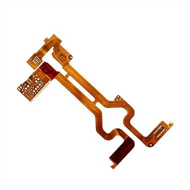
Description
We actively grasp the market trend and realize the strategic layout of the whole Automotive PCB Service Assembly, Oem Smart Electronics Printed Circuit Board, Doubled-sides Rigid-flex PCB industry chain. Continuous product improvement in terms of quality and technology is the only way we can compete aggressively in the marketplace. We are developing new strategies to make sure our company can keep up with the times and meet the principles of corporate social responsibility.
Product Detail

Quick Details
Model Number: Customize
Place of Origin: Shenzhen, China
Base Material: FR-4/aluminum/ceramic/cem-3/FR-1
Copper Thickness: 1/2OZ 1OZ 2OZ 3OZ
Board Thickness: 0.2-4mm
Min. Hole Size: 0.075mm/3mil
Min. Line Width: 0.1mm/4mil
Min. Line Spacing: 0.1mm/4mil
Surface Finishing: HASL
Certificate: ISO9001; TS16949
Other Service: PCB Design and layout
Solder mask color: Blue. green. red. black. white. etc
Layer: 1~24 Layers
Testing Service: AOI X-Ray Function Test

As an ISO9001 certificated electronics assembly manufacturer, adheres to a thorough quality and process control. The tests and inspections include physical and visual inspections, open & short tests, AOI inspections, X-ray inspection, and In-Circuit tests. We also make ageing testing both for mother board and finished product. These PCBA inspection process ensure customers final product meets their design specifications, and also control the whole production lot to high non-defective ratio which reduce the entire lead time.

Steps involved in the PCB assembly process
There are many steps involved in the PCBA and manufacturing process. To get the best quality final product, follow these steps:
Step 1: Add Solder Paste: This is the very initial stage of the assembly process. At this stage, solder paste is added to the component pads wherever soldering is required. Put the solder paste on the pads and stick it in the right place with the help of the solder screen. This screen is made from a PCB file with holes.
Step 2: Placing Components: With the solder paste added to the component pads, it's time to place the components. The PCB goes through a machine that precisely places these components on the pads. The tension provided by the solder paste holds the component in place.
Step 3: Reflow Oven: This step is used to permanently attach the components to the board. After the components are placed on the board, the PCB is passed through the reflow oven conveyor. The controlled heat of the oven melts the solder added in the first step, permanently connecting the components.
Step 4: Wave Soldering: In this step, the PCB is passed through a wave of molten solder. This will create an electrical connection between the solder, the PCB pads and the component leads.
Step 5: Cleaning: At this step, all the soldering process is completed. During the soldering process, a large amount of flux residue forms around the solder joint. As the name suggests, this step involves cleaning flux residues. Clean flux residue with deionized water and solvent. With this step, the PCB assembly is completed. Subsequent steps will ensure that the assembly is done correctly.
Step 6: Testing: At this stage, the PCB assembly is complete and inspections begin to test the placement of the components. This can be performed in two ways:
a. Manual: This inspection is usually done for smaller components, the number of components does not exceed one hundred.
b. Automatic: This check is performed to check for bad joints, wrong components, misplaced components, etc.
Product craft requirements:
1. Offset requirement: When the side is offset, the minimum connection width (C) shall not be less than 3/4 of the component weld end width (W) or pad width (P); calculated by the smaller of P and W.
2. Solder requirements: the minimum climbing tin height is greater than 1/3 of the castle.
3. component requirements: the minimum climbing tin height is greater than 1/3 of the castle.
4. Do not accept alternative materials.
5. PCB requirements: bare board shipment does not accept foaming or stratification.
6. PCBA requirements: anti-static full package
7. Cleaning requirements: special cleaning fluid, please note the water flow should be soft, not too fierce, carefully brush with a soft brush while brushing, both sides of the board should be operated with the same way.
As an experienced supplier, our company is the best choice for your ideal and cost-effective and high quality High Precision Microcomputer Double Pulse Spot Welder for Battery Welding. We will provide day and night service and constantly improve service. We uphold the faith of sincerity, carry forward the spirit of concentration, innovation and dedication, and realize the leap forward development. The company integrates advanced technology and experience at home and abroad, and is committed to developing more high-quality products.
Hot Tags: double-sided household breakers PCB assembly, China, suppliers, manufacturers, factory, customized, buy, cheap, quotation, low price, free sample, Cheap Flex PCB Online Prototype, Rigid Flex PCB Circuit Boards, Consumer Electronics Prototype PCB Assembly, Multilayer Industrial Control PCB Assembly, Industrial Control PCB Assembly, Medical Electronics PCB Assembly